Our Research Topics
- non-invasive clinical diagnostic tools
- sensor system development for precision agriculture
- novel microelectromechanical (MEMS) devices
- nanotechnology manufacturing methods
- biodefense applications
- new materials for MEMS/NEMS applications
- mechanical and bioinstrumentation design
- bioinformatics and machine learning approaches for data analysis
Nanotechnology Manufacturing Methods
Nanotechnology involves the study and creation of structures on the nanometer (nm) scale. A variety of tools have been developed in the last decade to achieve manufacturing structures on this length scale, including the nanoimprint lithography technique.
Nanoimprint lithography (NIL) is a novel technique that allows fabrication of sub-micron features into substrates using a modified embossing method into a polymer resist. In most cases, a stamp is produced by direct e-beam writing into a resist and then the pattern is etched into the substrate. Other stamp fabrication methods exist, but in general they are expensive to produce. When performing NIL, damage may occur to the stamp unless the process steps are optimized.
We illustrate a simple and inexpensive method to produce a test stamp to use for NIL process optimization. This may have wide applications in both industrial and academic settings.
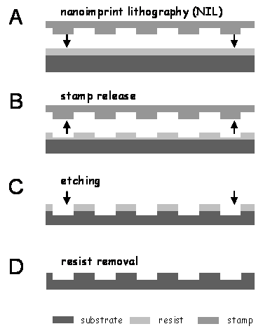
The NIL process consists of several fundamental process steps. (A) A stamp contains nanoscale physical structures. The stamp is physically brought into contact with a polymer resist on a substrate. (B) The stamp is pressed into the polymer, which results in imprints complementary to the stamp image. The polymer resist is cross-linked. (C) The stamp is withdrawn, and the substrate is etched. (D) Finally, the resist is stripped from the substrate. [from our paper: Yaghmaie F, Nielsen W, Han H, Bhushan A, Davis CE*. (2009) A simplified method to produce a functional test stamp for nanoimprint lithography (NIL). IEEE Sensors Journal 9(3): 233-234.]
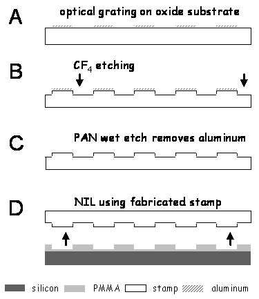
A stamp was produced from a commercial optical grating by the process shown below. We then applied the stamp to a 200 nm PMMA layer on a silicon substrate, and we were able to transfer the image. Using our inexpensive test stamp, we were able to optimize the NIL process, and we can expand our process capabilities into novel resists in the future.
Process flow to generate stamp. (A) The native optical grating is a high quality SiO2 substrate with an extremely thin layer of aluminum in nanometer sized line widths. The metal lines are geometrically arranged to diffract light; however, in our case, we use the metal as a mask. (B) The grating is etched using CF4, which begins to remove the oxide substrate between the metal lines. (C) A PAN (phosphoric, acetic, and nitric acid) wet etch removes the aluminum. (D) The modified grating now represents an NIL stamp.
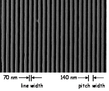
Creation of poly(methyl methacrylate) (PMMA) structures using the novel stamp. This test structure has a 70 nm line width with 140 nm pitch.
Commercial NIL stamps that are custom ordered may cost as much as ~$20,000 in some cases, and even home-made stamps are often time consuming and difficult to fabricate. These expensive stamps are just as likely to suffer damage during NIL process optimization as inexpensive ones, through mechanical force and stiction problems. By producing high quality test stamps from common starting materials, we can simplify NIL process characterization without risking damage to our primary stamps. Using relatively simple methods, it is possible to produce high quality NIL stamps by converting a commercial optical grating chip.