Our Research Topics
- non-invasive clinical diagnostic tools
- sensor system development for precision agriculture
- novel microelectromechanical (MEMS) devices
- nanotechnology manufacturing methods
- biodefense applications
- new materials for MEMS/NEMS applications
- mechanical and bioinstrumentation design
- bioinformatics and machine learning approaches for data analysis
New Materials for MEMS/NEMS Applications
By creating new materials for microsystems, we open new doors for future devices to be developed. Hybrid organic-inorganic films have attracted substantial attention in recent years in part due to the advantages of combining both organic and inorganic materials, and the possibility that devices made from these structures can be easily manufactured using existing semiconductor fabrication processes.
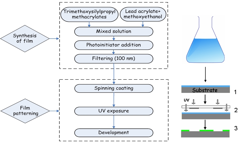
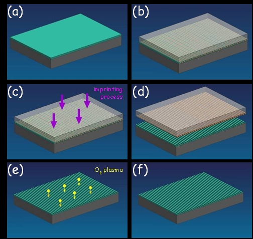
We have developed a new class of these materials using a unique solution spin-casting-based formulation. Below is a schematic illustrating the film synthesis and patterning processes. The solution based mixture is created and applied to substrates using a spin-coating process, and a photoactive compound in the solution generates free-radicals in response to UV exposure. The monomeric precursors rapidly polymerize to create micropatterns for final inorganic-organic device structures. [from our paper: Han H, Sutherland A, Yaghmaie F, Davis CE*. (2009) Development of a lead oxide photopatternable organic-inorganic film. Applied Physics Letters 94(14): 144106.]
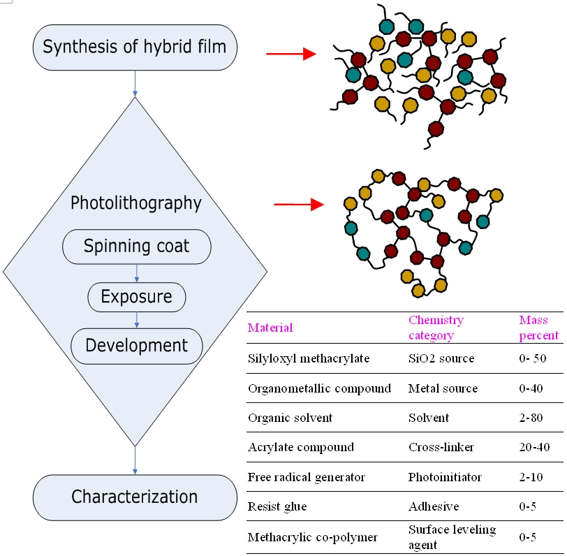
Below we show the typical process. The flowchart (left) represents the entire development process of the film from the solution-based synthesis to final characterization of the hybrid thin films. The solution content information (right)illustrates the typical solution components. [from our paper: Han H, Bissell J, Yaghmaie F, Davis CE*. (2010) Polymeric acrylate-based hybrid films containing lead and iron patterned by UV photo-polymerization. Langmuir 26(1): 515-520.]
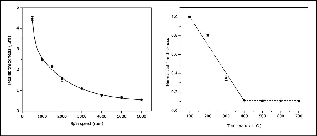
Due to the solution based nature of the thin film material, we can easily adjust the film thickness by altering the viscosity or the the spinning speed and annealing temperature of the processed film (the thickness is normalized). (left) The film thickness can be controlled as a function of the application spin speed. (right) Film thickness changes with annealing temperature. [from our paper: Han H, Bissell J, Yaghmaie F, Davis CE*. (2010) Polymeric acrylate-based hybrid films containing lead and iron patterned by UV photo-polymerization. Langmuir 26(1): 515-520.]
After demonstrating this initially with lead (Pb), we went on to adjust the composition to include: nickel (Ni), cobalt (Co) and iron (Fe). [from our paper: Bhushan A, Han H, Sutherland A, Boehme S, Yaghmaie F, Davis CE*. (2010) Generation of paramagnetic hybrid inorganic/organic thin films. Applied Organometallic Chemistry 24(7): 530-532.]
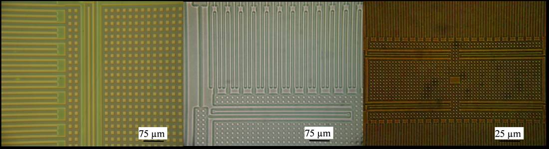
Post-processing and residual resist removal with plasma cleaning leaves behind a metal containing feature (in this case nickle). [from our paper: Bhushan A, Han H, Sutherland A, Boehme S, Yaghmaie F, Davis CE*. (2010) Generation of paramagnetic hybrid inorganic/organic thin films. Applied Organometallic Chemistry 24(7): 530-532.]
For all of our unique thin film formulations, we use a technique termed energy dispersive X-ray spectroscopy (EDX) to determine the elemental composition of the films. [from our paper: Bhushan A, Han H, Sutherland A, Boehme S, Yaghmaie F, Davis CE*. (2010) Generation of paramagnetic hybrid inorganic/organic thin films. Applied Organometallic Chemistry 24(7): 530-532.]
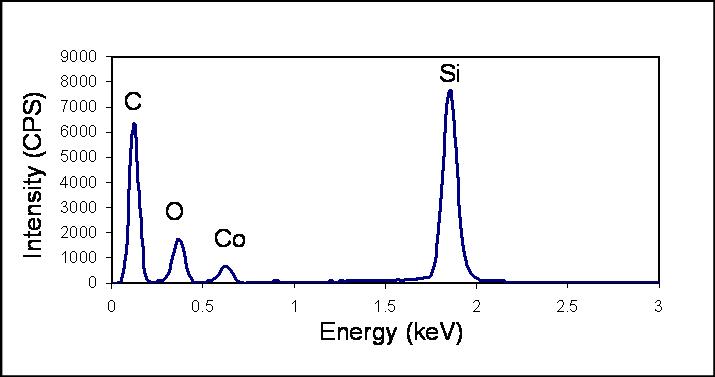
We also have shown that direct thermal-UV nanoimprinting of our organometallic hybrid film can be used to fabricate nanoscale features into the novel organic-inorganic solution containing our selected metals. The film can be patterned at low temperature and pressure, and requires only a short processing time. When analyzed by energy dispersion X-ray spectroscopy, we observe both organic and metal content in the final patterned features. We also observed that film thermal stability increases after UV and oxygen plasma treatments, which may lead to devices that perform well across a wide spectrum of temperatures. [from our paper: Han H, Bhushan A, Yaghmaie F, Davis CE*. (2010) Direct thermal-UV nanoimprint of an iron-containing organometallic hybrid film. Journal of Vacuum Science and Technology - Part B 28(1): 78-81.]
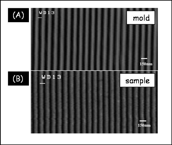
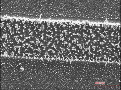
The direct nanoimprinting process successfully replicated nanometer scale patterns into our hybrid film. The original mold features were confirmed using a scanning electron microscope to ensure that the pattern is replicated faithfully into the film. We observed that the mold pitch is 144 nm, the line spacing was equally distributed across the surface, and the linewidth was 72 nm. When imprinted into our hybrid material, the mold features are effectively transferred, although the dimension of the line appears to be slightly wider than that of the space. The slightly broader linewidth may be a result of trapped air or trapped moisture present during the rapid nanoimprinting process. Further process optimization could alleviate this effect and could be explored prior to commercial use. [from our paper: Han H, Bhushan A, Yaghmaie F, Davis CE*. (2010) Direct thermal-UV nanoimprint of an iron-containing organometallic hybrid film. Journal of Vacuum Science and Technology - Part B 28(1): 78-81.]